This is Part 3 of the ESP8266 nEXT EVO Analog Extension Board (AN1)
In this part we will talk about the ESP8266 nEXT Evo 8 Bit I/O Expansion Port based on the PCF8574 chip from NXP, testing procedures and software programming for the AN1 Board
Previous related Articles:
- New ESP8266 DevBoard - CBDB nEXT EVO - General presentation, schematics, PCB, etc
- Part 2 - ESP8266 DevBoard - CBDB nEXT EVO - Firmware upload
- SSD1306 OLED Display for ESP8266 nEXT EVO Board
- ESP8266 nEXT EVO - Analog Extension Board - Part 1 - General view, schematics, PCB, etc
- ESP8266 nEXT EVO - Analog extension Board - Part 2 - I2C Bus Protocol, scanbus example.etc
--------------------------------------------------------------------------------------------------------------------------
For any new CBDB orders/requests please feel free to use as usual:
tech at esp8266-projects.com.
ESP8266 nEXT Evo bare PCB has also been made available directly at Dirty PCBs, our preferred PCB House for experimenting (**):
http://dirtypcbs.com/view.php?share=9699&accesskey=91d782fd4a10943fd36ecc371c7ff2cd
(**) - Actually you have there 2 Boards for the price of one, a ESP8266 nEXT Evo together with a AN1 nEXT Analog Extension Board that brings you a 18Bit ADC (autoscale 0-40V input!), 4x12Bit DAC, Precison Temperature measurement, 8bit I/O port, etc.
-------------------------------------------------------------------------------------------------------------------------
PCF8574 General Description
The PCF8574/74A provides general-purpose remote I/O expansion via the two-wire
bidirectional I2C-bus (serial clock (SCL), serial data (SDA)).
The devices consist of eight quasi-bidirectional ports, 100 kHz I2C-bus interface, three
hardware address inputs and interrupt output operating between 2.5 V and 6 V. The
quasi-bidirectional port can be independently assigned as an input to monitor interrupt
status or keypads, or as an output to activate indicator devices such as LEDs. System
master can read from the input port or write to the output port through a single register.
The active LOW open-drain interrupt output (INT) can be connected to the interrupt logic
of the microcontroller and is activated when any input state differs from its corresponding
input port register state. It is used to indicate to the microcontroller that an input state has
changed and the device needs to be interrogated without the microcontroller continuously
polling the input register via the I2C-bus.
Features :
- I2C-bus to parallel port expander
- 100 kHz I2C-bus interface (Standard-mode I2C-bus)
- Operating supply voltage 2.5 V to 6 V with non-overvoltage tolerant I/O held to VDD with 100uA current source
- 8-bit remote I/O pins that default to inputs at power-up
- Latched outputs directly drive LEDs
- Total package sink capability of 80 mA
- Active LOW open-drain interrupt output
- Eight programmable slave addresses using three address pins
- Low standby current (2.5 uA typical)
- -40C to +85C operation
- ESD protection exceeds 2000 V HBM per JESD22-A114 and 1000 V CDM per JESD22-C101
- Latch-up testing is done to JEDEC standard JESD78 which exceeds 100 mA
- Packages offered: DIP16, SO16, SSOP20
 |
| Bidirectional I/O Expander Example |
Something to remember:
- PCF8574 can SINK but NOT SOURCE much current - 100uA only (it cannot output high, if you want). Look at the above example how is connected the LED for SINKING current.
- Each of the 8 GPIOs have a minimum guaranteed sinking current of 10 mA per bit at 5 V.
- Each pin needs its own limiting resistor to prevent damage to the device!! keep under 25mA/pin.
- Maximum device limit sink current in about 80mA. If you need more, look after PCA8574 (200mA max sink current!)
For more details please take a look at the PCF8574 Datasheet
For easy testing the PCF8574 8Bit Port Output Pins we will use a very simple "Ghetto-Tester" based on 8 LED's and corresponding current limiting resitors:
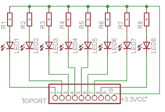
What we will need:
- ESP8266 nEXT EVO Board
- ESP8266 nEXT EVO - Analog Extension Board - AN1
- 8 LED Port Tester as described above
- For programming and uploading the driver and the software we will continue to use the LuaUploader as before.
Connection with the ESP8266 nEXT EVO Board is very easy, as Analog Extension Board - AN1 connector is fully compatible with the nEXT connector. Depending on how to you choose you socket type, you can install it on TOP or Bottom of the ESP8266 nEXT EVO Board :

By default, on the AN-1 Board you should have the following available devices:
- PCF8574 8Bit I/O Extension port - at address 0x20
- LM75 Temperature sensor - at address 0x48
- MCP4728 - 4x12Bit DAC - at address 0x60
- MCP3421 - 18Bit ADC - at address 0x68
A first step in testing the AN-1 available functions and devices will be to scan the nEXT I²C Bus and see if all the existing ones are alive and responding to the I²C Master requests. Also will list any new added devices, if alive.
Using the SCANBUS program described in the Part 2 of the AN-1 Series, you can find very easy if your PCF8574 8Bit I/O Extension port is available on the nEXT Bus :

Software implementation
PCF8574 8Bit I/O port is a quasi-bidirectional I/O Port, same as Port 1,2,3 on the 8051 MCU, if you like.
A quasi-bidirectional I/O is an input or output port without using a direction control register.
Whenever the master reads the register, the value returned to master depends on the
actual voltage or status of the pin. At power on, all the ports are HIGH with a weak 100 uA
internal pull-up to VDD, but can be driven LOW by an internal transistor, or an external
signal. The I/O ports are entirely independent of each other, but each I/O octal is controlled by the same read or write data byte.
Advantages of the quasi-bidirectional I/O over totem pole I/O include:
- Better for driving LEDs since the p-channel (transistor to VDD) is small, which saves die size and therefore cost. LED drive only requires an internal transistor to ground, while the LED is connected to VDD through a current-limiting resistor. Totem pole I/O have both n-channel and p-channel transistors, which allow solid HIGH and LOW output levels without a pull-up resistor — good for logic levels.
- Simpler architecture — only a single register and the I/O can be both input and output at the same time. Totem pole I/O have a direction register that specifies the port pin direction and it is always in that configuration unless the direction is explicitlychanged.
- Does not require a command byte. The simplicity of one register (no need for the pointer register or, technically, the command byte) is an advantage in some embedded systems where every byte counts because of memory or bandwidth limitations.
Testing I/O Port Output
There is only one register to control four possibilities of the port pin: Input HIGH, input
LOW, output HIGH, or output LOW.
- Input HIGH: The master needs to write 1 to the register to set the port as an input mode if the device is not in the default power-on condition. The master reads the register to check the input status. If the external source pulls the port pin up to VDD or drives logic 1, then the master will read the value of 1.
- Input LOW: The master needs to write 1 to the register to set the port to input mode if the device is not in the default power-on condition. The master reads the register to check the input status. If the external source pulls the port pin down to VSS or drives logic 0, which sinks the weak 100uA current source, then the master will read the value of 0.
- Output HIGH: The master writes 1 to the register. There is an additional ‘accelerator’ or strong pull-up current when the master sets the port HIGH. The additional strong pull-up is only active during the HIGH time of the acknowledge clock cycle. This accelerator current helps the port’s 100uA current source make a faster rising edge into a heavily loaded output, but only at the start of the acknowledge clock cycle to avoid bus contention if an external signal is pulling the port LOW to VSS/driving the port with logic 0 at the same time. After the half clock cycle there is only the 100uA current source to hold the port HIGH.
- Output LOW: The master writes 0 to the register. There is a strong current sink transistor that holds the port pin LOW. A large current may flow into the port, which could potentially damage the part if the master writes a 0 to the register and an external source is pulling the port HIGH at the same time.
 | |
| Simple quasi-bidirectional I/O example |
In our case, to light-up our LED's we will use the last option, Output LOW!
1. Init I2C bus/interface
-- init I2C nEXT BUS
function i2c_init()
i2c.setup(id, sda, scl, i2c.SLOW)
end
2. Set PCF8574 PORT Register Function
function setPort( port, stat)
i2c.start(id)
i2c.address(id, dev_addr ,i2c.TRANSMITTER)
i2c.write(id,stat)
i2c.stop(id)
end
3. Set Port function
Just a nicer way to write data to PCF8574 Register. Remember that we need to write a "ZERO" to the corresponding bit. We are sinking not sourcing !!
function setPortdata(p)
pp = 255-p
setPort(0x20,pp)
end
4. Main Program
i2c_init()
-- Direct port bit by bit set
setPortdata(0) -- All OFF
setPortdata(1) -- P0 - ON
setPortdata(2) -- P1 - ON
setPortdata(4) -- P2 - ON
setPortdata(8) -- P3 - ON
setPortdata(16) -- P4 - ON
setPortdata(32) -- P5 - ON
setPortdata(64) -- P6 - ON
setPortdata(128) -- P7 - ON
-- mixed bit set - set 2 or more bits at the same time. Do not exceed max sink current!
setPortdata(3) -- P0 & P1 - ON
-- test autoincrement bit
i=1
tmr.alarm( 0, 200, 1, function()
print(i)
setPortdata(i)
i=i+i
if i>128 then i=1
end
end)
tmr.stop(0)
-- cycle visual step-by-step, from left-to-right
port={1,2,4,8,128,64,32,16}
i=1
tmr.alarm( 0, 100, 1, function()
print(port[i])
setPortdata(port[i])
i=i+1
if i>8 then i=1
end
end)
-- Knight Rider style test - anybody remember about Knight Rider KITT car?:)
port={1,2,4,8,128,64,32,16}
i=1
c=1
tmr.alarm( 0, 75, 1, function()
--print(port[i])
setPortdata(port[i])
if c<8 then i=i+1
else
if c>14 then
c=1
i=2
else
i=i-1
end
end
--print(port[i].." i="..i.." c="..c)
c=c+1
end)
That's all for today, next time, PCF8574 Input, and a nice 4x4 Matrix Keyboard example :)