ESP8266 Projects Blog
Home of CBDB / MPDMv4 /SmartMon Development boards (ESP-12/ESP-07).
Guidelines and ESP8266 programming examples using LUA, Eclipse and Arduino IDE, ESP Basic and many more!
WARNING!! You will play with LIVE MAINS!! Deadly zone!!
If you don't
have any experience and are not qualified for working with MAINS power I
will not encourage you to play arround!. The
author take no responsibility for any injury or
death resulting, directly or indirectly, from your inability to
appreciate the hazards of household mains voltages.
The circuit diagrams are as accurately as possible, but are offered with no
guarantees whatsoever.
There is no guarantee that this design meets any Rules which may be in
force in your country so please check before your local
rules/regulations.
For any new orders/requests please feel free to use as usual: tech (at) esp8266-projects.com. MPDMv4 Boards are also available on Tindie: AC MAINS Dimmer - MPDMv4
For today we have a short but comprehesive Tutorial on how to drive the MPDMv4 AC MAINS Dimmer board using the Arduino IDE:
Arduino IDE code example for the Youtube Video Tutorial:
/* Dimmer
Demonstrates the sending data from the computer to the Arduino board, in this case to control the brightness of MPDMv4 AC MAINS Dimmer. The data is sent in individual bytes, each of which ranges from 0 to 255. Arduino reads these bytes and uses them to set the VCNT brightness command .
The circuit: MPDMv4 Board attached from digital pin 3 to ground. Serial connection to Processing, Max/MSP, or another serial application
created 2006 by David A. Mellis modified 30 Aug 2011 by Tom Igoe and Scott Fitzgerald modified 14 Apr 2016 by TJ for esp8266-projects.com AC MAINS Power Dimmer MPDMv4 Driver This example code is in the public domain.
http://www.arduino.cc/en/Tutorial/Dimmer
*/
const int vcntPin = 3; // the pin that the MPDMv4 VCNT pin is attached to
void setup() { // initialize the serial communication: Serial.begin(9600); // initialize the VCNTPin as an output: pinMode(vcntPin, OUTPUT); // set default brightness value analogWrite(vcntPin, 230); }
void loop() { byte brightness;
// check if data has been sent from the computer: if (Serial.available()) { // read the most recent byte (which will be from 0 to 255): brightness = Serial.parseInt(); Serial.print("Command received : "); Serial.println(brightness); // set the brightness of the LED: analogWrite(vcntPin, brightness); } }
For programming and uploading the driver and the software we will continue to use the LuaUploader as before.
ADC Frontend description
Selection of the input voltage divider is done using an analog switch driven by PCF8574 PORT P0 and P1 bits: 0 - 1:20 Divider 1 - 1:10 Divider 2 - 1:5 Divider 3 - Full Voltage Range
As the ADC Input is programmed to be used in the 0-2V range that will give us the followings available ranges:
0 -> 0 - 40V 1 -> 0 - 20V 2 -> 0 - 10V 3 -> 0 - 2V In the case of using the MCP3421 ADC at 12 Bit resolution, we will have the following corresponding LSB values:
- 1:20 Divider - 0.02V - 1:10 Divider - 0.01V - 1:5 Divider - 0.005V - Full Range - 0.001V
Software implementation 1. Init I2C bus/interface
Standard I2C Bus Initialisation function:
function init_I2C() i2c.setup(bus, sda, scl, i2c.SLOW) end
2. Set PCF8574 PORT Register Function
function setPort( port, stat) i2c.start(id) i2c.address(id, dev_addr ,i2c.TRANSMITTER) i2c.write(id,stat) i2c.stop(id) end
3. Set Port function
Just a nicer way to write data to PCF8574 Register. Remember that we
need to write a "ZERO" to the corresponding bit. We are sinking not
sourcing !!
function setPortdata(p) pp = 255-p setPort(0x20,pp) end
4. Set Voltage Divider function
Select the desired Voltage divider ratio based on the choosen ratio value and calibrated LSB data.
function SetVDivider(rtio) if (rtio==0) then xrt=x20 end if (rtio==1) then xrt=x10 end if (rtio==2) then xrt=x5 end if (rtio==3) then xrt=xfl end print("XRT = "..xrt) setPortdata(rtio) -- select desired voltage divider return xrt end
-- Set/Change Voltage Divider ratio:
SetVDivider(0) -- 1:20 Divider SetVDivider(1) -- 1:10 Divider SetVDivider(2) -- 1:5 Divider SetVDivider(3) -- 1:1 Full Voltage in!!
5. MAIN Program
-- Main Program id = 0 sda=2 --GPIO4 scl=1 --GPIO5 dev_addr = 0x20
MCP4726 - 12 Bit I2C DAC Driver for ESP8266 nEXT EVO AN-1
Youtube Video here
From today we will move on the Analog interface part of the nEXT EVO Board AN-1 and we will start talking about the Digital to Analog conversion, Analog Autoscaling input and Analog to Digital conversion .
For the Digital to Analog conversion part the choosen one is the Microchip MCP4728 I2C DAC IC.
The MCP4728 device is a quad, 12-bit voltage output Digital-to-Analog Convertor (DAC) with non-volatile memory (EEPROM).
As it has a on-board precision output amplifier with rail-to-rail analog output swing capabilities that means first of all that we don't need any other Output Buffer as mandatory needed for non-buffered DAC's.
The MCP4728 device has also a high precision internal voltage reference (VREF = 2.048V). The user can select the internal reference or external reference (VDD) for each channel individually.
Features
• 12-Bit Voltage Output DAC with 4 Buffered Voltage Outputs
- Each output is driven by its own output buffer with a gain of 1 or 2 depending on the gain and
VREF selection bit settings.
- In
normal mode, the DC impedance of the output pin is about 1Ω. In
Power-Down mode,
the output pin is internally connected to 1 kΩ, 100 kΩ,
or 500 kΩ, depending on the
Power-Down selection bit settings.
- The VOUT pin can drive up to 1000 pF of capacitive load. It is recommended to use a load
with RL greater than 5 kΩ.
• On-Board Non-Volatile Memory (EEPROM) for DAC Codes and I2CTM Address Bits
• Internal or External Voltage Reference Selection
• Output Voltage Range:
- Using Internal VREF (2.048V):
0.000V to 2.048V with Gain Setting = 1
0.000V to 4.096V with Gain Setting = 2
- Using External VREF (VDD): 0.000V to VDD
• ±0.2 LSB DNL (typical)
• Fast Settling Time: 6 μs (typical)
• Normal or Power-Down Mode
• Low Power Consumption
• Single-Supply Operation: 2.7V to 5.5V
• I2C Interface:
- Address bits: User Programmable to EEPROM
- Standard (100 kbps), Fast (400 kbps) and High Speed (3.4 Mbps) Modes
• 10-Lead MSOP Package
• Extended Temperature Range: -40°C to +125°C
In
this part we will continue talking about the ESP8266 nEXT Evo 8 Bit I/O Expansion
Port based on the PCF8574 chip from NXP, testing procedures and
software programming for the AN1 Board.
After testing the Output of the 8Bit I/O Port it's now time to test also the Input function.
So, what can be easier to use for such a processs than some pushbuttons for interaction? I was thinking about some sort of buttons interface and because I just have arround a small 4x4 Matrix Keyboard why not directly a keyboard interface, especially that I'm waiting to receive some very thin membrane ones to be used for some projects.
-------------------------------------------------------------------------------------------------------------------------- For any new CBDB orders/requests please feel free to use as usual: tech at esp8266-projects.com.
(**)
- Actually you have there 2 Boards for the price of one, a ESP8266 nEXT
Evo together with a AN1 nEXT Analog Extension Board that brings you a
18Bit ADC (autoscale 0-40V input!), 4x12Bit DAC, Precison Temperature
measurement, 8bit I/O port, etc. -------------------------------------------------------------------------------------------------------------------------
4x4 Matrix Keyboard connected to the ESP8266 nEXT Evo Board 8Bit I/O Expansion Port
For more details and explanations please take a look at the Youtube Video from above: https://youtu.be/cVv7GCHmZ_o
Software implementation
For a better understanding of the way how the PCF8574 8Bit quasi-bidirectional I/O Port is working it might be a good idea to look at the prevoius related article and the PCF8574 Datasheet
1. Init I2C bus/interface -- init I2C nEXT BUS function i2c_init() i2c.setup(id, sda, scl, i2c.SLOW) end
2. Set PCF8574 PORT Register Function
function setPort( port, stat) i2c.start(id) i2c.address(id, dev_addr ,i2c.TRANSMITTER) i2c.write(id,stat) i2c.stop(id) end
3. Set Port function
Just a nicer way to write
data to PCF8574 Register. Remember that we need to write a "ZERO" to
the corresponding bit. We are sinking not sourcing !!
function setPortdata(p) pp = 255-p setPort(0x20,pp) end
4. I/O Port READ Input
function read_input(dev_addr) i2c.start(id) i2c.address(id, dev_addr,i2c.RECEIVER) c = i2c.read(id,1) d = 255-string.byte(c) i2c.stop(id) --print("Read Value : "..d) return c,d end
5. OLED DISPLAY Related Functions
5.1 Init OLED Display
function init_OLED(sda,scl) --Set up the u8glib lib sla = 0x3C i2c.setup(0, sda, scl, i2c.SLOW) disp = u8g.ssd1306_128x64_i2c(sla) disp:setFont(u8g.font_6x10) disp:setFontRefHeightExtendedText() disp:setDefaultForegroundColor() disp:setFontPosTop() disp:setRot180() end
5.2 Print TEXT on Display
function PrintText() disp:drawStr(10, 25, str1) disp:drawStr(105, 25, str2) end
5.3 Print_LCD Function
function print_LCD() disp:firstPage() repeat PrintText() disp:drawFrame(2,2,126,62) until disp:nextPage() == false end
while j<5 do if d==port[i]+row[j] then print("Col[i] = "..port[i]) -- for debug only print("Row[j] = "..row[j]) -- for debug only print("Read Value : "..d) --for debug only print("Read Key : "..k) -- for debug only print("Pressed KEY Value : "..key[k].."\n") -- print pressed KEY value str2=key[k] print_LCD() -- print also on Display end j=j+1 k=k+1 tmr.wdclr() end j=1
i=i+1 if i>4 then i=1 end if k>16 then k=1 end end)
In this part we will talk about the ESP8266 nEXT Evo 8 Bit I/O Expansion Port based on the PCF8574 chip from NXP, testing procedures and
software programming for the AN1 Board
-------------------------------------------------------------------------------------------------------------------------- For any new CBDB orders/requests please feel free to use as usual: tech at esp8266-projects.com.
(**)
- Actually you have there 2 Boards for the price of one, a ESP8266 nEXT
Evo together with a AN1 nEXT Analog Extension Board that brings you a
18Bit ADC (autoscale 0-40V input!), 4x12Bit DAC, Precison Temperature
measurement, 8bit I/O port, etc. -------------------------------------------------------------------------------------------------------------------------
PCF8574 General Description The PCF8574/74A provides general-purpose remote I/O expansion via the two-wire bidirectional I2C-bus (serial clock (SCL), serial data (SDA)).
The devices consist of eight quasi-bidirectional ports, 100 kHz I2C-bus interface, three hardware address inputs and interrupt output operating between 2.5 V and 6 V. The quasi-bidirectional port can be independently assigned as an input to monitor interrupt status or keypads, or as an output to activate indicator devices such as LEDs. System master can read from the input port or write to the output port through a single register.
The active LOW open-drain interrupt output (INT) can be connected to the interrupt logic of the microcontroller and is activated when any input state differs from its corresponding input port register state. It is used to indicate to the microcontroller that an input state has changed and the device needs to be interrogated without the microcontroller continuously polling the input register via the I2C-bus.
Features :
I2C-bus to parallel port expander
100 kHz I2C-bus interface (Standard-mode I2C-bus)
Operating supply voltage 2.5 V to 6 V with non-overvoltage tolerant I/O held to VDD with 100uA current source
8-bit remote I/O pins that default to inputs at power-up
Latched outputs directly drive LEDs
Total package sink capability of 80 mA
Active LOW open-drain interrupt output
Eight programmable slave addresses using three address pins
Low standby current (2.5 uA typical)
-40C to +85C operation
ESD protection exceeds 2000 V HBM per JESD22-A114 and 1000 V CDM per JESD22-C101
Latch-up testing is done to JEDEC standard JESD78 which exceeds 100 mA
Packages offered: DIP16, SO16, SSOP20
Bidirectional I/O Expander Example
Something to remember:
PCF8574 can SINK but NOT SOURCE much current - 100uA only (it cannot output high, if you want). Look at the above example how is connected the LED for SINKING current.
Each of the 8 GPIOs have a minimum guaranteed sinking current of 10 mA per bit at 5 V.
Each pin needs its own limiting resistor to prevent damage to the device!! keep under 25mA/pin.
Maximum device limit sink current in about 80mA. If you need more, look after PCA8574 (200mA max sink current!)
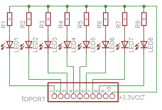
For easy testing the PCF8574 8Bit Port Output Pins we will use a very simple "Ghetto-Tester" based on 8 LED's and corresponding current limiting resitors:
A first step in testing the AN-1 available functions and devices will
be to scan the nEXT I²C Bus and see if all the existing ones are alive
and responding to the I²C Master requests. Also will list any new added devices, if alive.
Using the SCANBUS program described in the Part 2 of the AN-1 Series, you can find very easy if your PCF8574 8Bit I/O Extension port is available on the nEXT Bus :
Software implementation
PCF8574 8Bit I/O port is a quasi-bidirectional I/O Port, same as Port 1,2,3 on the 8051 MCU, if you like.
A quasi-bidirectional I/O is an input or output port without using a direction control register.
Whenever the master reads the register, the value returned to master depends on the
actual voltage or status of the pin. At power on, all the ports are HIGH with a weak 100 uA
internal pull-up to VDD, but can be driven LOW by an internal transistor, or an external
signal. The I/O ports are entirely independent of each other, but each I/O octal is controlled by the same read or write data byte.
Advantages of the quasi-bidirectional I/O over totem pole I/O include:
Better for driving LEDs since the p-channel (transistor to VDD) is small, which saves die size and therefore cost. LED drive only requires an internal transistor to ground, while the LED is connected to VDD through a current-limiting resistor. Totem pole I/O have both n-channel and p-channel transistors, which allow solid HIGH and LOW output levels without a pull-up resistor — good for logic levels.
Simpler architecture — only a single register and the I/O can be both input and output at the same time. Totem pole I/O have a direction register that specifies the port pin direction and it is always in that configuration unless the direction is explicitlychanged.
Does not require a command byte. The simplicity of one register (no need for the pointer register or, technically, the command byte) is an advantage in some embedded systems where every byte counts because of memory or bandwidth limitations.
Testing I/O Port Output
There is only one register to control four possibilities of the port pin: Input HIGH, input
LOW, output HIGH, or output LOW.
Input HIGH: The master needs to write 1 to the register to set the port as an input mode if the device is not in the default power-on condition. The master reads the register to check the input status. If the external source pulls the port pin up to VDD or drives logic 1, then the master will read the value of 1.
Input LOW: The master needs to write 1 to the register to set the port to input mode if the device is not in the default power-on condition. The master reads the register to check the input status. If the external source pulls the port pin down to VSS or drives logic 0, which sinks the weak 100uA current source, then the master will read the value of 0.
Output HIGH: The master writes 1 to the register. There is an additional ‘accelerator’ or strong pull-up current when the master sets the port HIGH. The additional strong pull-up is only active during the HIGH time of the acknowledge clock cycle. This accelerator current helps the port’s 100uA current source make a faster rising edge into a heavily loaded output, but only at the start of the acknowledge clock cycle to avoid bus contention if an external signal is pulling the port LOW to VSS/driving the port with logic 0 at the same time. After the half clock cycle there is only the 100uA current source to hold the port HIGH.
Output LOW: The master writes 0 to the register. There is a strong current sink transistor that holds the port pin LOW. A large current may flow into the port, which could potentially damage the part if the master writes a 0 to the register and an external source is pulling the port HIGH at the same time.
Simple quasi-bidirectional I/O example
In our case, to light-up our LED's we will use the last option, Output LOW!
1. Init I2C bus/interface -- init I2C nEXT BUS function i2c_init() i2c.setup(id, sda, scl, i2c.SLOW) end
2. Set PCF8574 PORT Register Function
function setPort( port, stat) i2c.start(id) i2c.address(id, dev_addr ,i2c.TRANSMITTER) i2c.write(id,stat) i2c.stop(id) end
3. Set Port function
Just a nicer way to write data to PCF8574 Register. Remember that we need to write a "ZERO" to the corresponding bit. We are sinking not sourcing !!
function setPortdata(p) pp = 255-p setPort(0x20,pp) end
4. Main Program
i2c_init()
-- Direct port bit by bit set setPortdata(0) -- All OFF setPortdata(1) -- P0 - ON setPortdata(2) -- P1 - ON setPortdata(4) -- P2 - ON setPortdata(8) -- P3 - ON setPortdata(16) -- P4 - ON setPortdata(32) -- P5 - ON setPortdata(64) -- P6 - ON setPortdata(128) -- P7 - ON
-- mixed bit set - set 2 or more bits at the same time. Do not exceed max sink current! setPortdata(3) -- P0 & P1 - ON
-- test autoincrement bit i=1 tmr.alarm( 0, 200, 1, function() print(i) setPortdata(i) i=i+i if i>128 then i=1 end end)
tmr.stop(0)
-- cycle visual step-by-step, from left-to-right port={1,2,4,8,128,64,32,16} i=1 tmr.alarm( 0, 100, 1, function() print(port[i]) setPortdata(port[i]) i=i+1 if i>8 then i=1 end end)
-- Knight Rider style test - anybody remember about Knight Rider KITT car?:) port={1,2,4,8,128,64,32,16} i=1 c=1 tmr.alarm( 0, 75, 1, function() --print(port[i]) setPortdata(port[i]) if c<8 then i=i+1 else if c>14 then c=1 i=2 else i=i-1 end end --print(port[i].." i="..i.." c="..c) c=c+1 end)
In this part we will talk a bit about the nEXT Bus I²C
protocol and we will
start also a longer, multi-part discussion about testing procedures and
software programming for the AN1 Board devices and functions (I/O
Expansion port, Temperature, ADC, DAC, Voltage measurements,etc.
-------------------------------------------------------------------------------------------------------------------------- For any new CBDB orders/requests please feel free to use as usual: tech at esp8266-projects.com.
(**)
- Actually you have there 2 Boards for the price of one, a ESP8266 nEXT
Evo together with a AN1 nEXT Analog Extension Board that brings you a
18Bit ADC (autoscale 0-40V input!), 4x12Bit DAC, Precison Temperature
measurement, 8bit I/O port, etc. -------------------------------------------------------------------------------------------------------------------------
Today topic
First let's have a very quick look at the nEXT bus protocol: I²C What is I²C?
I²C (Inter-Integrated Circuit), pronounced I-squared-C, is a multi-master, multi-slave, single-ended, two-wired serial bus - SDA (data line) and SCL (clock line) - invented by Philips Semiconductor (now NXP Semiconductors). It is typically used for attaching lower-speed peripheral ICs to processors and microcontrollers.
Features of the I2C-bus:
Only two bus lines are required; a serial data line (SDA) and a serial clock line (SCL).
Each device connected to the bus is software addressable by a unique address and simple master/slave relationships exist at all times; masters can operate as master-transmitters or as master-receivers.
It is a true multi-master bus including collision detection and arbitration to prevent data corruption if two or more masters simultaneously initiate data transfer.
Serial, 8-bit oriented, bidirectional data transfers can be made at up to 100 kbit/s in the Standard-mode, up to 400 kbit/s in the Fast-mode, up to 1 Mbit/s in Fast-mode Plus, or up to 3.4 Mbit/s in the High-speed mode.
Serial, 8-bit oriented, unidirectional data transfers up to 5 Mbit/s in Ultra Fast-mode
On-chip filtering rejects spikes on the bus data line to preserve data integrity.
The number of ICs that can be connected to the same bus is limited only by a maximum bus capacitance. More capacitance may be allowed under some conditions.
SDA and SCL signals
Both SDA and SCL are bidirectional lines, connected to a positive supply voltage via a current-source or pull-up resistor:
When the bus is free, both lines are HIGH. The output stages of devices connected to the bus must have an open-drain or open-collector to perform the wired-AND function. Data on the I²C-bus can be transferred at rates of up to 100 kbit/s in the Standard-mode, up to 400 kbit/s in the Fast-mode, up to 1 Mbit/s in Fast-mode Plus, or up to 3.4 Mbit/s in the High-speed mode. The bus capacitance limits the number of interfaces connected to the bus.
For a single master application, the master’s SCL output can be a push-pull driver design if there are no devices on the bus which would stretch the clock.
SDA and SCL logic levels
Due to the variety of different technology devices (CMOS, NMOS, bipolar) that can be connected to the I²C-bus, the levels of the logical ‘0’ (LOW) and ‘1’ (HIGH) are not fixed and depend on the associated level of VDD.
Input reference levels are set as 30 % and 70 % of VDD; VIL is 0.3VDD and VIH is 0.7VDD.
Timing Diagram for F/S-mode devices on the I²C-bus
Some legacy device input levels were fixed at VIL= 1.5 V and VIH= 3.0 V, but all new devices require this 30 %/70 % specification.
For a more deep and extensive I²C protocol undestanding ( Data Validity, START and STOP conditions, Byte format, Acknowledge (ACK) and Not Acknowledge (NACK), Clock synchronisation, etc,etc please take a look at the official NXP I²C Protocol datasheet. I²C protocol it is quite a serious separate topic to discuss :).
Before going further with our main topic I will insist only one one more thing, as it looks it creates a lot of confusion sometime:
The slave address and R/W Bit (7 bit mode)
Data transfers follow the format shown in the picture below:
A full data transfer
After the START condition (S), a slave address is sent. This address is seven bits long followed by an eighth bit which is a data direction bit (R/W) — a ‘zero’ indicates a transmission (WRITE), a ‘one’ indicates a request for data (READ):
The first byte after the START procedure
A data transfer is always terminated by a STOP condition (P) generated by the master.
However, if a master still wishes to communicate on the bus, it can generate a repeated START condition (Sr) and address another slave without first generating a STOP condition. Various combinations of read/write formats are then possible within such a transfer:
Master-transmitter transmits to slave-receiver. The transfer direction is not changed and the slave receiver acknowledges each byte:
Master reads slave immediately after first byte. At the moment of the first acknowledge, the master-transmitter becomes a master-receiver and the slave-receiver becomes a slave-transmitter. This first acknowledge is still generated by the slave. The master generates subsequent acknowledges. The STOP
condition is generated by the master, which sends a not-acknowledge (A)
just before the STOP condition:
Combined format. During a change of direction within a transfer, the START condition and the slave address are both repeated, but with the R/W bit reversed. If a master-receiver sends a repeated START condition, it sends a not-acknowledge (A) just before the repeated START condition:
Now, after a very brief (very!) I²C protocol presentation, let's go back to our Analog Extension Board:
ESP8266 nEXT EVO + AN-1 Boards
First thing that we want to do, after the AN-1 Board is properly soldered, cleaned, visual inspection OK, etc, will be to tests it and validate it as a proper working Board.
A fist step in testing the AN-1 available functions and devices will
be to scan the nEXT I²C Bus and see if all the existing ones are alive
and responding to the I²C Master requests. Also will list any new added devices, if alive.
1. Find device function
function find_dev(i2c_id, dev_addr) i2c.start(i2c_id) c=i2c.address(i2c_id, dev_addr ,i2c.TRANSMITTER) i2c.stop(i2c_id) return c end
2. Scan Bus for devices function
function scanbus() i2c.setup(id,sda,scl,i2c.SLOW) for i=1,127 do if find_dev(id, i)==true then if i==32 then print("- PCF8574 8Bit I/O Extension port - found at address 0x"..string.format("%02X",i).." -> "..i) else if i==72 then print("- LM75 Temperature sensor - found at address 0x"..string.format("%02X",i).." -> "..i) else if i==96 then print("- MCP4728 - 4x12Bit DAC - found at address 0x"..string.format("%02X",i).." -> "..i) else if i==104 then print("- MCP3421 - 18Bit ADC - found at address 0x"..string.format("%02X",i).." -> "..i) else if i==60 then print("- SSD1306 OLED Display - found at address 0x"..string.format("%02X",i).." -> "..i) else print("- NEW UNREGISTERED DEVICE - found at address 0x"..string.format("%02X",i).." -> "..i) end end end end end end tmr.wdclr() end end
3. MAIN Scanbus Program
id=0 sda=2 scl=1 scanbus()
Next time we will continue with deeper testing and programming for each AN-1 available device/function.
 MPDMv4 by ESP8266-Projects.com is licensed under a Creative Commons Attribution-NonCommercial 4.0 International License.