ESP8266 Projects Blog
Home of CBDB / MPDMv4 /SmartMon Development boards (ESP-12/ESP-07).
Guidelines and ESP8266 programming examples using LUA, Eclipse and Arduino IDE, ESP Basic and many more!
PCF8591 Module like the one from here or here, advertised as new versions.
For programming and uploading the driver and the software we will use the ESPBasic
Connection with the ESP8266 nEXT EVO Board is very easy, asPCF8591 Moduleconnector
is fully compatible with the nEXT Bus connector.
Driver implementation As been a I2C compatible device you need to have a standard I2C Bus Initialisation function as usual and also to know the I2C address of the device. For a detailed PCF 8591 Control Byte description go to PART1.
Software:
1. Main program:
let address = 72 'PCF8591 I2C Address i2c.setup(4,5) 'choose your I2C bus pins
cls let dac = 0 let dac_v = 0 let adc0_1 = 0 let adc0_v = 0 let v_cal = 0.0128
ESP Basic series - I2C driver example for the PCF8591 I2C 8-bit A/D and D/A converter. General view:
The PCF8591 is a single-chip, single-supply low-power 8-bit CMOS data acquisition device with four analog inputs, one analog output and a serial I2C-bus interface. Three address pins A0, A1 and A2 are used for programming the hardware address, allowing the use of up to eight devices connected to the I2C-bus without additional hardware. Address, control and data to and from the device are transferred serially via the two-line bidirectional I2C-bus.
The functions of the device include analog input multiplexing, on-chip track and hold function, 8-bit analog-to-digital conversion and an 8-bit digital-to-analog conversion. The maximum conversion rate is given by the maximum speed of the I2C-bus.
Features:
Single power supply
Operating supply voltage 2.5 V to 6.0 V
Low standby current
Serial input and output via I2C-bus
I2C address selection by 3 hardware address pins
Max sampling rate given by I2C-bus speed
4 analog inputs configurable as single ended or differential inputs
PCF8591 Module like the one from here or here, advertised as new versions.
For programming and uploading the driver and the software we will use the ESPBasic
Connection with the ESP8266 nEXT EVO Board is very easy, asPCF8591 Moduleconnector
is fully compatible with the nEXT Bus connector.
Driver implementation
As been a I2C compatible device you need to have a standard I2C Bus Initialisation function as usual and also to know the I2C address of the device.
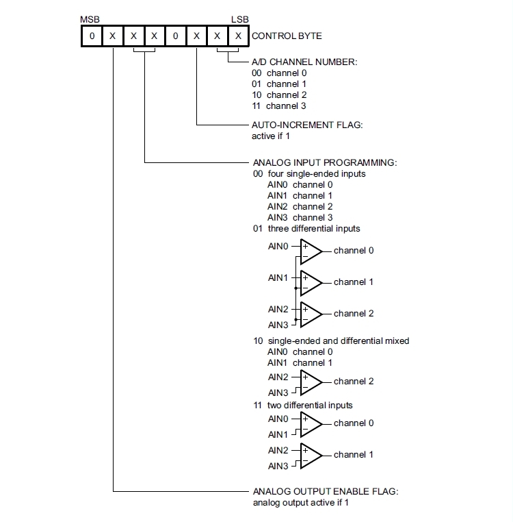
Control Byte is the second byte sent to a PCF8591 device and is stored in its control register and is required to control the device function :
Things to take care about:
The upper nibble of the control register is used for enabling the analog output, and for programming the analog inputs as single-ended or differential inputs. The lower nibble selects one of the analog input channels defined by the upper nibble .
If the auto-increment flag is set, the channel number is incremented automatically after each A/D conversion. If the auto-increment mode is desired in applications where the internal oscillator is used, the analog output enable flag must be set in the control byte (bit 6). This allows the internal oscillator to run continuously, by this means preventing conversion errors resulting from oscillator start-up delay.
The analog output enable flag can be reset at other times to reduce quiescent power consumption.
The selection of a non-existing input channel results in the highest available channel number being allocated. Therefore, if the auto-increment flag is set, the next selected channel is always channel 0.
The most significant bits of both nibbles are reserved for possible future functions and must be set to logic 0. After a Power-On Reset (POR) condition, all bits of the control register are reset to logic 0. The D/A converter and the oscillator are disabled for power saving. The analog output is switched to a high-impedance state.
Software:
1. Main program:
let address = 72 'PCF8591 I2C Address i2c.setup(4,5) 'choose your I2C bus pins cls let dac = 0 let dac_v = 0 let v_cal = 0.0128 wprint " <b>PCF8591 - 8-bit A/D and D/A converter driver <br>DAC demo</b><br><i>by tech@esp8266-projects.com</i><br><br> " wprint " Input DAC value" textbox dac button " Set Value ",[SetDAC] wprint " <br>DAC Output (V)" textbox dac_v wprint "<br><br>" button " Stop Program", [Exit] wait
In the ESP Basic Web editor interface Type & Save your program as "PCF8591.bas" and Run it.
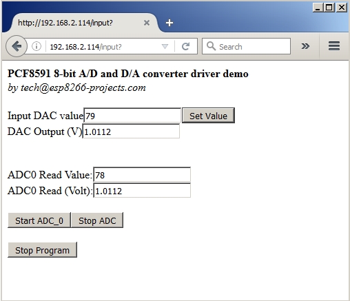
If all OK the result should look as below:
If you want your program to start automatically at reboot/power ON then just Save it as "default.bas" and also from Settings Tab enable the "Run default.bas at startup".
Be aware that at start-up/reboot, it is a delay before your program will start automatically.
In the next part about PCF8591 we will talk about the ADC Driver implementation.
The main goal of the project is to create a AC Mains Light dimmer that can automatically control the level of light and keep in in the desired set interval without any external intervention.
Why would you be intrested in such a setup? Well, if you have any interest in hydroponics, photography, or anywhere where you need some sort of constant flood light lamps with precise light intensitity level setup then might be a good idea to take a look :) What we will need:
BH1750FVI Module . Can be ordered in packs of ONE, FIVE or even TEN from the corresponding links. My 10 one was backordered but received it quite quickly.
For programming and uploading the driver and the software we will continue to use the LuaUploader as before.
Connection with the ESP8266 nEXT EVO Board is very easy, as MPU6050 GY-521 Module connector
is fully compatible with the nEXT Bus connector. Depending on how to you
choose you socket type, you can install it on TOP or Bottom of the ESP8266 nEXT EVO Board :
BH1750FVI Module directly connected to the ESP8266 nEXT EVO Board
And the whole project setup, with MPDVv4 AC Dimmer connected on ESP8266 GPIO13 (pin 7):
MPDM v4 + nEXT EVO + BH1750FVI
Closer look, MPDMv4 connected at ESP8266 GPIO13 (Pin7) for PWM control
function set_light() read_input(dev_addr) ll = light - hst --lower level lh = light + hst --upper level if (lux < ll) then p=0 i = i - step if (i<0) then i = 0 end pwm.setduty(7, i) end if (lux >lh) then p=0 i = i + step if (i>880) then i = 880 end pwm.setduty(7, i) end --print("Auto Level Adjust : "..i) --print(ll) --print(lh) if (ll< lux and lux < lh) then if (p<1) then p=1 end if (p<2) then print(string.format("\nLight Level: %0.2f lux",lux)) print("Auto Level Adjust : "..i) p=2 end end end
Main Program --PWM testing for MPDMv4 AC Dimmer Board
In the process of choosing of some Light Sensors for one of the new projects that will involve the nEXT EVO Board and also the MPDMv4 Mains Dimmer somebody suggested to give a try also to the ROHM BH1750FVI Sensor.
As you can see on the picture above, on the tiny board, you have the BH1750FVI Sensor, a LDO regulator some filtering caps and pull-up resistors and that's it!
BH1750FVI Module - Bottom
The bottom side is bringing us more good news, the Module interface connector is fully compatible with the nEXT EVO Bus!
BH1750FVI Overview
BH1750FVI is an digital Ambient Light Sensor IC for I2C bus interface. This IC is the mostly used to obtain the ambient light data for adjusting LCD and Keypad backlight power of Mobile phone. This is great as we are looking forward to use it for Automatic light adjustment using the MPDMv4 AC Dimmer board :)
Features
I2C bus Interface ( f / s Mode Support )
Spectral responsibility is approximately human eye response
Illuminance to Digital Converter
Wide range and High resolution. ( 1 - 65535 lx )
Low Current by power down function
50Hz / 60Hz Light noise reject-function
1.8V Logic input interface
Native 3.3V Device
No need any external parts
Light source dependency is little. ( ex. Incandescent Lamp. Fluorescent Lamp. Halogen Lamp. White LED. Sun Light )
It is possible to select 2 type of I2C slave-address.
Adjustable measurement result for influence of optical window ( It is possible to detect min. 0.11 lx, max. 100000 lx by using this function. )
Small measurement variation (+/- 20%)
The influence of infrared is very small.
Internal Diagram
BH1750FVI - Internal Diagram
PD - Photo diode with approximately human eye response.
AMP - Integration-OPAMP for converting from PD current to Voltage.
ADC - AD converter for obtainment Digital 16bit data.
Logic + I2C Interface :
- Ambient Light Calculation and I2C BUS Interface. It is including below register.
- Data Register - This is for registration of Ambient Light Data. Initial Value is
"0000_0000_0000_0000".
- Measurement Time Register - This is for registration of measurement time. Initial Value
is "0100_0101".
OSC - Internal Oscillator ( typ. 320kHz ). It is CLK for internal logic.
BH1750FVI Module from above. Can be ordered in packs of ONE, FIVE or even TEN from the corresponding links. My 10 one was backordered but received it quite quickly.
For programming and uploading the driver and the software we will continue to use the LuaUploader as before.
Connection with the ESP8266 nEXT EVO Board is very easy, as MPU6050 GY-521 Module connector
is fully compatible with the nEXT Bus connector. Depending on how to you
choose you socket type, you can install it on TOP or Bottom of the ESP8266 nEXT EVO Board :
BH1750FVI Module directly connected to the ESP8266 nEXT EVO Board
BH1750FVI Driver implementation
1. Init I2C bus/interface
Standard I2C Bus Initialisation function:
function init_I2C() i2c.setup(bus, sda, scl, i2c.SLOW) end
2. WRITE Function - Set BH1750FVI Register config
From BH1750FVI Datasheet :
No active state : pwr_down 0x00
Wating for measurment command : pwr_on=0x01
Reset data register value - not accepted in POWER_DOWN mode : reset=0x07
Continuous modes, no pwr down:
Start measurement at 1lx resolution. Measurement time is approx 120ms:
hi_res_m1=0x10
Start measurement at 0.5lx resolution. Measurement time is approx 120ms.
hi_res_m2=0x11
Start measurement at 4lx resolution. Measurement time is approx 16ms.
lo_res_m1=0x13
Device is automatically set to Power Down after measurement:
Start measurement at 1lx resolution. Measurement time is approx 120ms.
hi_res_m3=0x20
Start measurement at 0.5lx resolution. Measurement time is approx 120ms.
hi_res_m4=0x21
Start measurement at 1lx resolution. Measurement time is approx 120ms.
lo_res_m2=0x23
function setcfg(cfg) i2c.start(id) i2c.address(id, dev_addr ,i2c.TRANSMITTER) i2c.write(id,cfg) i2c.stop(id) end
For any new orders/requests please feel free to use as usual: tech at esp8266-projects.com. MPDMv4 Boards are also available on Tindie: AC MAINS Dimmer - MPDMv4
WARNING!! You will play with LIVE MAINS!! Deadly zone!!
If you don't
have any experience and are not qualified for working with MAINS power I
will not encourage you to play arround!. The
author take no responsibility for any injury or
death resulting, directly or indirectly, from your inability to
appreciate the hazards of household mains voltages.
The circuit diagrams are as accurately as possible, but are offered with no
guarantees whatsoever.
There is no guarantee that this design meets any Rules which may be in
force in your country so please check before your local
rules/regulations.
One of the main problem that people has been complained about was the fact that a simple MAINS Power Dimmer/Switch unit like the basic one presented last year is using sometime too much resources from a already overloaded application MCU/processor:
MPDMv3 - MAINS Dimmer/Switch with Phase detection
One of the scenarios, directly related with ESP8266 is about the limited timers capabilities that you have. For example, if you want to implement a proper web server to directly serve your webpages from ESP8266 you are automatically using one timer. If you want to start using the second one for your ZCD processing ...well...it's becoming very tricky. Very.
Don't uderstand me wrong, a bigger, better MCU can do it probably very well,
but even then if you have the chance to free some resources easily, do
it!. And I really cannot see a ESP8266 acting as a App MCU (webserver,
data logger, MQTT client, etc, etc) and doing reliable also other demanding
functions as Processing Zero Crossing Detection.
SOLUTION?
I can see only one, and it is a lesson learned many years ago: keep your real-time processing functions away from your Application MCU/Processor. To do that we just need to move the ZCD processing function from the ESP8266/whatever MCU you want to the MPDM Driver itself:
MPDMv4 - MAINS Phase detection and ZCD processing
What means that? means that in this new configuration our ESP8266 will be free from any type of real-time ZCD processing that is related with the MAINS Dimming process, you just need to send to the MPDMv4 driver a voltage (Vcontrol) in a pre-established range (0-3V for example) that will correspond with different desired Dimming levels.
What we have obtained? A UNIVERSAL MAINS Power Dimmer driver that can be used with any MCU you might want or even no MCU at all. You can dimm it even with a simple Potentiometer at input, no programming, no code, no nothing!!
Legend:
PURPLE - Phase detector output
BLUE - Reversed phase signal (normalised)
Yellow - Triac Driver CMD signal (PWM)
Vcontrol = 0, CMD Duty cycle=6%
Vcontrol = 2V, CMD Duty=50%
Vcontrol = 2.8V, CMD Duty=96%
How can be done that? Easy. Use PWM or a DAC, your choice. For ESP8266 I will recommend you to use a DAC, like the MCP4726 or, why not , the MCP4728, for a full 4 Channel MAINS Dimmers solution. PWM in case of the ESP8266..let's say that is has some limitations that you will discover very soon that you don't like :)
The mains advantages of using DAC?
Notable:
1. Very low to zero overhead on the App MCU
2. High precision (DAC from above are 12 bit!! - 4096 levels of dimming!!)
3. You can use the "set-and-forget" technique using DAC internal nonvolatile memory (EEPROM) and have the same level on the next power-off/on cycle.
IMPLEMENTATION
SCHEMATICS
As the only functional difference between the previous MPDMv3 MAINS Dimmer and the new MPDMv4 is the presence of the ZCD function onboard, basically, without some small bits and pieces around like the MOV protection circuit, you can see it exactly as it is: a MPDMv3 with a ZCD circuit onboard:
MPDMv3 - Phase detection and Triac control
Zero crossing detector circuit
MPDMv4 PCB:
MPDMv4 PCB
As you can see from the above picture, it was carefully designed with proper MAINS isolation from the rest of the driver, you can see even the extra isolation slots done for a even bigger Creepage distance.
And because I know this terms still creates some confusion, short definitions below:
CLEARANCE is the shortest distance in air between two conductive parts. CREEPAGE distance means the shortest distance along the surface of a solid insulating material between two conductive parts.
A creepage distance cannot be less than the associated clearance so that
the shortest creepage distance possible is equal to the required
clearance. However, there is no physical relationship, other than this
dimensional limitation, between the minimum clearance in air and the
minimum acceptable creepage distance.
And the new, freshly baked result:
MPDMv4 - MAINS Power Dimmer/Switch with Phase detection and ZCD Processing
Next time we will move on to the Software side, to see what is going on with our Webserver interface & stuff.
For programming and uploading the driver and the software we will continue to use the LuaUploader as before.
ADC Frontend description
Selection of the input voltage divider is done using an analog switch driven by PCF8574 PORT P0 and P1 bits: 0 - 1:20 Divider 1 - 1:10 Divider 2 - 1:5 Divider 3 - Full Voltage Range
As the ADC Input is programmed to be used in the 0-2V range that will give us the followings available ranges:
0 -> 0 - 40V 1 -> 0 - 20V 2 -> 0 - 10V 3 -> 0 - 2V In the case of using the MCP3421 ADC at 12 Bit resolution, we will have the following corresponding LSB values:
- 1:20 Divider - 0.02V - 1:10 Divider - 0.01V - 1:5 Divider - 0.005V - Full Range - 0.001V
Software implementation 1. Init I2C bus/interface
Standard I2C Bus Initialisation function:
function init_I2C() i2c.setup(bus, sda, scl, i2c.SLOW) end
2. Set PCF8574 PORT Register Function
function setPort( port, stat) i2c.start(id) i2c.address(id, dev_addr ,i2c.TRANSMITTER) i2c.write(id,stat) i2c.stop(id) end
3. Set Port function
Just a nicer way to write data to PCF8574 Register. Remember that we
need to write a "ZERO" to the corresponding bit. We are sinking not
sourcing !!
function setPortdata(p) pp = 255-p setPort(0x20,pp) end
4. Set Voltage Divider function
Select the desired Voltage divider ratio based on the choosen ratio value and calibrated LSB data.
function SetVDivider(rtio) if (rtio==0) then xrt=x20 end if (rtio==1) then xrt=x10 end if (rtio==2) then xrt=x5 end if (rtio==3) then xrt=xfl end print("XRT = "..xrt) setPortdata(rtio) -- select desired voltage divider return xrt end
-- Set/Change Voltage Divider ratio:
SetVDivider(0) -- 1:20 Divider SetVDivider(1) -- 1:10 Divider SetVDivider(2) -- 1:5 Divider SetVDivider(3) -- 1:1 Full Voltage in!!
5. MAIN Program
-- Main Program id = 0 sda=2 --GPIO4 scl=1 --GPIO5 dev_addr = 0x20
MCP4726 - 12 Bit I2C DAC Driver for ESP8266 nEXT EVO AN-1
Youtube Video here
From today we will move on the Analog interface part of the nEXT EVO Board AN-1 and we will start talking about the Digital to Analog conversion, Analog Autoscaling input and Analog to Digital conversion .
For the Digital to Analog conversion part the choosen one is the Microchip MCP4728 I2C DAC IC.
The MCP4728 device is a quad, 12-bit voltage output Digital-to-Analog Convertor (DAC) with non-volatile memory (EEPROM).
As it has a on-board precision output amplifier with rail-to-rail analog output swing capabilities that means first of all that we don't need any other Output Buffer as mandatory needed for non-buffered DAC's.
The MCP4728 device has also a high precision internal voltage reference (VREF = 2.048V). The user can select the internal reference or external reference (VDD) for each channel individually.
Features
• 12-Bit Voltage Output DAC with 4 Buffered Voltage Outputs
- Each output is driven by its own output buffer with a gain of 1 or 2 depending on the gain and
VREF selection bit settings.
- In
normal mode, the DC impedance of the output pin is about 1Ω. In
Power-Down mode,
the output pin is internally connected to 1 kΩ, 100 kΩ,
or 500 kΩ, depending on the
Power-Down selection bit settings.
- The VOUT pin can drive up to 1000 pF of capacitive load. It is recommended to use a load
with RL greater than 5 kΩ.
• On-Board Non-Volatile Memory (EEPROM) for DAC Codes and I2CTM Address Bits
• Internal or External Voltage Reference Selection
• Output Voltage Range:
- Using Internal VREF (2.048V):
0.000V to 2.048V with Gain Setting = 1
0.000V to 4.096V with Gain Setting = 2
- Using External VREF (VDD): 0.000V to VDD
• ±0.2 LSB DNL (typical)
• Fast Settling Time: 6 μs (typical)
• Normal or Power-Down Mode
• Low Power Consumption
• Single-Supply Operation: 2.7V to 5.5V
• I2C Interface:
- Address bits: User Programmable to EEPROM
- Standard (100 kbps), Fast (400 kbps) and High Speed (3.4 Mbps) Modes
• 10-Lead MSOP Package
• Extended Temperature Range: -40°C to +125°C