Showing posts with label ADC. Show all posts

Monday, November 14, 2016

Mailbag - PCF8591 I2C 8 bit ADC/DAC Driver - Part 2


ESP Basic series -  I2C driver example for the PCF8591 I2C 8-bit A/D and D/A converter - PART2

For a deeper description of the PCF8591 and simple DAC driver example please go to PART 1


 What we will need:


    Connection with the ESP8266 nEXT EVO Board is very easy, as PCF8591 Module connector is fully compatible with the nEXT Bus connector.


Driver implementation
As been a I2C compatible device you need to have a standard I2C Bus Initialisation function as usual and also to know the I2C address of the device.  
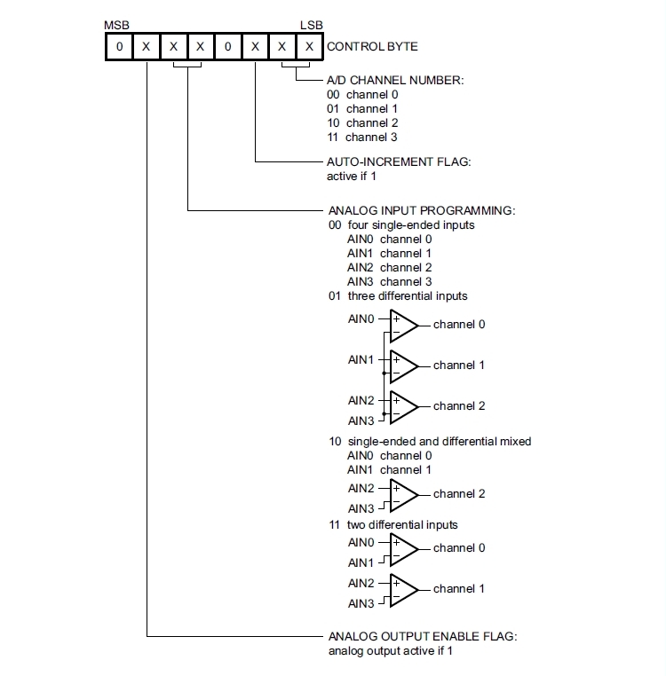
For a detailed PCF 8591 Control Byte description go to PART1.


Software: 

1. Main program: 
 
let address = 72   'PCF8591 I2C Address
i2c.setup(4,5)       'choose your I2C bus pins

cls
let dac = 0
let dac_v = 0
let adc0_1 = 0
let adc0_v = 0
let v_cal = 0.0128

adc0_1 = "ADC stopped"

wprint " <b>PCF8591 8-bit A/D and D/A converter driver demo</b><br><i>by tech@esp8266-projects.com</i><br><br> "

wprint " Input DAC value"
textbox dac

button " Set Value ",[SetDAC]

wprint " <br>DAC Output (V)"
textbox dac_v

wprint "<br>"

wprint "<br><br>ADC0 Read Value:"
textbox adc0_1

wprint "<br>ADC0 Read (Volt):"
textbox adc0_v
wprint "<br><br>"
 
button " Start ADC_0 ",[ADC0]
button " Stop ADC", [Exit ADC]

wprint "<br><br>"
button " Stop Program", [Exit]

wait


2. Set DAC subroutine: 

 [SetDAC]
dac_v = dac * v_cal

i2c.begin(address)
i2c.write(64)  'DAC Enable
delay 5
i2c.write(dac)
i2c.end()
wait


3. Enable ADC subroutine:

[ADC0]
timer 1000, [readADC]
wait


4. Read ADC subroutine:
 
[readADC]
ch = 64
i2c.begin(address)               'start another transaction
i2c.write(ch)                         'point to the ADC_0 - keep DAC ON
delay 5
i2c.end()                                'end write transaction

i2c.begin(address)                 'start another transaction
i2c.requestfrom(address,2)    'start a transaction to read 2 bytes
delay 5
adc0_0 = i2c.read()              'read the 1st byte
adc0_1 = i2c.read()              'read the 2nd byte
i2c.end()                                'end read transaction
adc0_v = v_cal + adc0_1 * v_cal
wait


5. EXIT ADC subroutine:
 
[Exit ADC]
timer 0
adc0_1 = "ADC stopped"
wait


6. Exit Program button subroutine:
 
[Exit]
timer 0
end


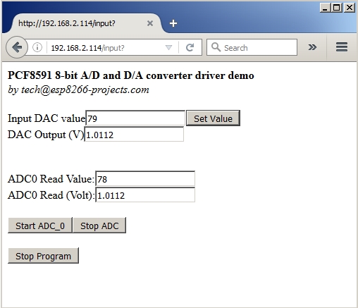
In the ESP Basic Web editor interface Type & Save your program as "PCF8591.bas" and Run it.  

If all OK the result should look as below:


Friday, November 11, 2016

Mailbag - PCF8591 I2C 8 bit ADC/DAC Driver - Part 1


ESP Basic series -  I2C driver example for the PCF8591 I2C 8-bit A/D and D/A converter.


General view:


   The PCF8591 is a single-chip, single-supply low-power 8-bit CMOS data acquisition
device with four analog inputs, one analog output and a serial I2C-bus interface. Three
address pins A0, A1 and A2 are used for programming the hardware address, allowing
the use of up to eight devices connected to the I2C-bus without additional hardware.
Address, control and data to and from the device are transferred serially via the two-line
bidirectional I2C-bus.
 

  The functions of the device include analog input multiplexing, on-chip track and hold
function, 8-bit analog-to-digital conversion and an 8-bit digital-to-analog conversion. The
maximum conversion rate is given by the maximum speed of the I2C-bus.


Features:

  • Single power supply
  • Operating supply voltage 2.5 V to 6.0 V
  • Low standby current
  • Serial input and output via I2C-bus
  • I2C address selection by 3 hardware address pins
  • Max sampling rate given by I2C-bus speed
  • 4 analog inputs configurable as single ended or differential inputs
  • Auto-incremented channel selection
  • Analog voltage range from VSS to VDD
  • On-chip track and hold circuit
  • 8-bit successive approximation A/D conversion
  • Multiplying DAC with one analog output.

For more details please take a look at the PCF8591 Datasheet


What we will need:

    Connection with the ESP8266 nEXT EVO Board is very easy, as PCF8591 Module connector is fully compatible with the nEXT Bus connector.


Driver implementation

As been a I2C compatible device you need to have a standard I2C Bus Initialisation function as usual and also to know the I2C address of the device.

Control Byte is the second byte sent to a PCF8591 device and is stored in its control register and is required to control the device function :


 Things to take care about: 

 The upper nibble of the control register is used for enabling the analog output, and for programming the analog inputs as single-ended or differential inputs. 
  The lower nibble selects one of the analog input channels defined by the upper nibble .

  If the auto-increment flag is set, the channel number is incremented automatically after each A/D conversion. If the auto-increment mode is desired in applications where the internal oscillator is used,
the analog output enable flag must be set in the control byte (bit 6). This allows the
internal oscillator to run continuously, by this means preventing conversion errors
resulting from oscillator start-up delay. 


  The analog output enable flag can be reset at other times to reduce quiescent power consumption.
 

   The selection of a non-existing input channel results in the highest available channel number being allocated. Therefore, if the auto-increment flag is set, the next selected channel is always channel 0. 

   The most significant bits of both nibbles are reserved for possible future functions and must be set to logic 0. After a Power-On Reset (POR) condition, all bits of the control register are reset to logic 0. 
   The D/A converter and the oscillator are disabled for power saving. 
   
  The analog output is switched to a high-impedance state.
 

Software: 

1. Main program: 
 
let address = 72 'PCF8591 I2C Address
i2c.setup(4,5) 'choose your I2C bus pins

cls
let dac = 0
let dac_v = 0
let v_cal = 0.0128

wprint " <b>PCF8591 - 8-bit A/D and D/A converter driver <br>DAC demo</b><br><i>by tech@esp8266-projects.com</i><br><br> "

wprint " Input DAC value"
textbox dac

button " Set Value ",[SetDAC]

wprint " <br>DAC Output (V)"
textbox dac_v

wprint "<br><br>"
button " Stop Program", [Exit]

wait


2. Set DAC subroutine: 

 
[SetDAC]
dac_v = dac * v_cal
i2c.begin(address)
i2c.write(64) 'Enable DAC
delay 5
i2c.write(dac)
i2c.end()
wait


3. EXIT program button:

[Exit]
timer 0
end


In the ESP Basic Web editor interface Type & Save your program as "PCF8591.bas" and Run it.  

 
If all OK the result should look as below:


If you want your program to start automatically at reboot/power ON then just Save it as "default.bas" and also from Settings Tab enable the "Run default.bas at startup".


Be aware that at start-up/reboot, it is a delay before your program will start automatically.


In  the next part about PCF8591 we will talk about the ADC Driver implementation.


Thursday, August 11, 2016

ESP8266 - Internal ADC 2 - the easy way example


This is just a very quick example on how to add a Voltage Divider to the ESP8266 Internal ADC input to increase the ADC input range.

For more theory behind, please take a look at the previous related article: ESP8266 - Internal ADC


Today project:

      Measure a voltage input range from 0-5V with the ESP8266 internal ADC


What do we need:

  • 2 Resistors for the voltage divider, R1=105.6k, R2=24.08k. I am using here precision resistors and the values are measured values with a proper calibrated bench meter.
  • a good, trustable, calibrated ok Multimeter.
  • some wires to connect all together.


I will not insist on connections, take a deeper look at the previous article about


Voltage divider schematic and Vout (ADC input voltage) formula


How do we do it :


1. Measure your Max desired input voltage
    In my case, Max Input Voltage (Vmax) = 5.1919 (measured)


2. Measure Resistors values:
    R1 = 105.6k
    R2 = 24.08k


3. Check if Full Scale Value at the voltage divider output is inside the ADC defined domain:
  • Calculated : Vout = (R2/(R1+R2))*Vin = 0.964072733 V
  • Measured = 0.96038V
     Good enough for the precision we are looking for. ESP8266 ADC is 10bit only and not exactly the most accurate in town


4. Calculate Voltage Divider Ratio:
  • Vdivider Ratio= Max Input Voltage/Fullscale value =  5.405976676


5.  Read ADC value : 
       adcr = adc.read(0)
      print("    ReadADC     : "..adcr)
     Average result for adcr = 1017

THIS IS IMPORTANT !! It tell us that we are inside the ADC domain as adcr < 1024 !

IF adcr > 1023 then you need to adjust your voltage divider resistors to fit inside ADC domain!


6. Calculate LSB  in 2 ways to cross check that we have the right value:
  • LSB = Input Voltage read by multimeter/ADC readed Value = 
                   =  5.1919 / 1017 =  0.005105113 V
      OR
  • LSB = (ADC Input  pin read Voltage by multimeter/ADC readed Value/)*Vdivider Ratio = 
                  = (0.96038/1017)*5.405976676 = 0.005105113 V
       It looks that we have the right LSB Value for our exercise!

     If you want to know also the ADC LSB, then
       LSB = ADC Input  pin read Voltage by multimeter/ADC readed Value  =   
                =  0.96038/1017 = 0.000944346 V

    Guess what's happening if you multiply ADC LSB with Vdivider ratio :)


7. Software Implementation for the ADC read function:

 function readADC()
      ad = 0
      LSB = 0.005105113 --calibrate based on your voltage divider AND Vref!
      adcr = adc.read(0)
      ad= adcr*LSB       
      print("    ReadADC     : "..adcr)
      print("    Read Voltage     : "..ad)
      return ad
end

and some results in the terminal window:

> SENT: readADC()
readADC()
    ReadADC     : 1017
    Read Voltage     : 5.191899921
>


Tuesday, June 2, 2015

Mailbag Arrival !! ACS712 Current Sensor Board


   Because of the very cheap ACS712 Current Sensor Board modules available all over the place, I really think that everybody heard about ACS712 sensor from Allegro MicroSystems.

  As I was asked if "Can be used as a current sensor module for our ESP8266 Projects without too much hustle?", I ordered few of them and let's explore them for the answer :)

   The ACS712 device consists of a precise, low-offset, linear Hall circuit with a copper conduction path located near the surface of the die. That means that it is a isolated path device, a very nice thing if you want to monitor MAINS Current or any other High Voltage path that you want isolated from your device.

IMPORTANT NOTE !!  This device is a Hall Effect transducer.  It should not be used near significant magnetic fields.  If you have a magnetic noisy environment take a look at other solutions like isolation transformers, isolation OpAmps, linear isolation circuit, bus path isolation, etc.


 Theory of operation 

 Applied current flowing through the ACS712 copper conduction path generates a magnetic field which the Hall IC converts into a proportional voltage. Device accuracy is optimized through the close proximity of the magnetic signal to the Hall transducer.
A precise, proportional voltage is provided by the low-offset, chopper-stabilized BiCMOS Hall IC, which is programmed for accuracy after packaging.

  The ACS712 outputs an analog signal, VIOUT that varies linearly with the uni- or bi-directional AC or DC primary sampled current, IP (between IP+ e IP-) within the range specified.

  It requires a power supply of 5V (VCC) and two capacitors to filter power supply and output.
CF is recommended for noise management, with values that depend on the application.

Typical application from the Datasheet: 


   ACS712 Current Board comes in 3 different models of this integrated circuit, depending on the maximum measured current : 5A  20  or  30A

5A Module20A Module30A Module
Supply Voltage (VCC)     5VDC     5VDC        5VDC
Measurement Range   -5 to +5 A   -20 to +20 A        -30 to +30 A
Voltage at 0A   VCC/2     VCC/2      VCC/2
Scale Factor   185 mV/A   100 mV/A      66 mV/A
Variant  ACS712ELC-05A   ACS712ELC-10A     ACS712ELC-30A


   For our today experiment, I will use the one below, a 100mV/A one:


What we will need:
  •  ACS712 Current Board module (pick your desired choice -  5A, 20A, 30A )
  • CBDB Board ( or any other ESP8266 Board you may like but who has the same capabilities)
  •  USB adapter (take a look on Part 1 for details about the USB Adapter 
  •  2 x 10 Ω /10 W  - Load resistors
  • Connection wires - various colors
  • Breadboard
  • Bench Power Supply 
  • Voltage Level Shifter and dc amplifier module - VLSAM DC(see details below)


Voltage Level Shifter and amplifier module - VLSAM DC

  As our main goal is to explore the posibility to use the ACS712 module with ESP8266 devices, from the description above and datasheet we can identify very quick some problems that need to be solved to make ACS712 a "ESP Friendly" device:

ASC712: 
  •  5 Vdc power supply device
  •  measure positive and negative 5/20/30Amps, corresponding to the analog output 100mV/A BUT
  • "ZERO" point, means no test current through the output voltage is VCC / 2 =5v/2=2.5V !

ESP8266:
  • 3V only device
  • ADC range  max: 0-1V

  What we will need is to "move" the "ZERO" point as low as we want to GND and in the same time to amplify the received analog signal to obtain a better resolution in the desired measuring range. (don't forget, for our experiment we have DC only voltage here and just one current flow direction)

   So, what can be done? 

Probably they are some other solutions to this problem, and if you know any of them, please feel free to share in the comments below, but the clasical one is to use a difference amplifier:


    This kind of amplifier uses both inverting and non-inverting inputs of a OPAmp with a gain of one to produce an output equal to the difference between the inputs. Actually if you take a closer look it is a special case of the differential amplifier.
   The good thing is that in the same time you can also choose the resistances values in a way to amplify the difference. 

    If all the resistor values are equal, this amplifier will have a differential voltage gain of 1. The analysis of this circuit is essentially the same as that of an inverting amplifier, except that the noninverting input (+) of the op-amp is at a voltage equal to a fraction of V2, rather than being connected directly to ground. As would stand to reason, V2 functions as the noninverting input and V1 functions as the inverting input of the final amplifier circuit. Therefore:

                  Vout = V2 - V1

    If we want to provide a differential gain of anything other than 1, we would have to adjust the resistances in both upper and lower voltage dividers, necessitating multiple resistor changes and balancing between the two dividers for symmetrical operation.

    A limitation of this simple amplifier design is the fact that its input impedances are rather low compared to that of some other op-amp configurations, most notably the noninverting (single-ended input) amplifier. Each input voltage source has to drive current through a resistance, which constitutes far less impedance than the bare input of an op-amp alone. It is a solution to this problem, fortunately, quite simple,  all we need to do is “buffer” each input voltage signal through a voltage follower.


   For our case, as we want to "substract" the ACS712 - 2.5Vdc to move the "ZERO" point near GND, we will have:
  • V1 = 2.5V - can be easy obtained from 5V with a buffered voltage divider
  • V2 = VIOUT - output voltage from ASC712 Module
  • Amplification:
    • IF R1=R2=R3=R4=10K 
      •  output for ADC input of 100mV/A
      • max range: 10A
      • resolution:  10mA
    • Changing range  R1=R2=10K, R3=R4=100k 
      • output for ADC input of 1V/A
      • max range: 1A
      • resolution: 1mA


VLSAM DC Schematic


And the simulation result for a 0-10A, 2.5-3.5 VIOut sweep:


  • GREEN      - Voltage divider output  : 2.5Vdc
  • FUCHSIA  -  ASC712 VIOut            : 2.5 -> 3.5Vdc
  • RED           -  ADC input                   : 0 -> 1Vdc


So far so good, let's move it on a breadboard for a quick test:


Monday, April 6, 2015

18 Bit ADC - MCP3421 - I2C Driver - ESP8266 CBDB


----------------------------------  UPDATE  --------------------------------------

For a ADC Input Frontend with Auto-range capabilities in the 0-40V Input range take a look also at the new ADC Input related article

---------------------------------  UPADTE  ----------------------------------------


    After testing the ESP8266 Internal ADC I think it's time to see also a higher resolution ADC at work. For this project we will use Microchip MCP3421 I2C ADC.

   The MCP3421 is a single channel, low-noise, high accuracy delta-sigma A/D converter with differential inputs and up to 18 bits of resolution in a small SOT-23-6 package. The on-board precision 2.048V reference voltage enables an input range of ±2.048V differentially. 
   The device uses a two-wire I2C compatible serial interface and operates from a single power supply ranging from 2.7V to 5.5V.  

    This device has an onboard programmable gain amplifier (PGA). User can select the PGA gain of x1, x2, x4, or x8 before the analog-to-digital conversion takes place.  This allows the MCP3421 device to convert a smaller input signal with high resolution. 

    The device has two possible to configure conversion modes:
  • Continuous mode
  • One-Shot mode. 
    In One-Shot mode, the device enters a low current standby mode automatically after one conversion. This reduces current consumption greatly during idle periods. Very goob for low power battery powered applications.

FEATURES: 
    • 18-bit resolution
    • Small 6-lead SOT-23 packaging
    • Differential input operation
    • On-board voltage reference with 5 ppm/°C drift
    • On-board PGA, gains of 1, 2, 4, 8
    • Programmable data rate options
      • 3.75 SPS (18 bits)
      • 15 SPS (16 bits)
      • 60 SPS (14 bits)
      • 240 SPS (12 bits)
    • INL 10 ppm of FSR max
    • Low current consumption, 145 µA at 3V
    • One-shot or continuous conversion options
    • Supports I2C™ serial interface
    • Extended temperature range: -40°C to +125°C

    For more details, please see MCP3421 Datasheet


    As been available in SOT-23-6 package, we will use again an DIP adaptor that will make it easy to integrate it on our CBDB Board expansion slots:

MCP3421 - SOT-23-6 To DIP Adapter

   Our CBDB Board has started to evolve and develop nice, with some interesting functions on board:


    Because of the high interest and the number of requests raised by the CBDB project in the next weeks we will run small batches of CBDB based devboard PCBs. The main purpose of the CBDB board was for local training and drivers development but  if any new one interested please express your wishes at: tech at esp8266-projects.com.

    It will be nothing fancy, just CBDB Board + some extra goodies on a standard 2 side factory made PCB that can help you to connect in minutes a new module and start programming. A nice I2C Dev Board, KISS concept at its plenitude :). 
A related Article will follow as soon as the first ones will hit the MailBox.

 
CBDB DevBoard v2.0b


    What we will need for our ADC project:
 

MCP3421 ADC I2C Driver implementation


    As MCP3421 has a I2C compatible compatible interface, driver building it following more or less the same  process  as before for I2C devices.
 
   Few important consideration about MCP3421: 

   The MCP3421 has an 8-bit wide configuration register to select for: PGA gain, conversion rate, and conversion mode. This register allows the user to change the operating condition of the device and check the status of the device operation. The user can rewrite the configuration byte any time during the device operation.

    The MCP3421 device accepts a fully differential analog input signal which is connected on the VIN+ and VINinput pins. The differential voltage that is converted is defined by VIN = (VIN+ - VIN-) where VIN+ is the voltage applied at the VIN+ pin and VIN- is the voltage applied at the VIN- pin. 
    The input signal level is amplified by the programmable gain amplifier (PGA) before the conversion.

    The digital output code produced by the MCP3421 is a function of PGA gain, input signal, and internal reference voltage. In a fixed setting, the digital output code is proportional to the voltage difference between the two analog inputs.
 

   The output data format is a binary two’s complement.
 

   With this code scheme, the MSB can be considered a sign indicator. When the MSB is a logic ‘0’, it indicates a positive value. When the MSB is a logic ‘1’, it
indicates a negative value. The following is an example of the output code: 
 
  •  for a negative full-scale input voltage: 100...000 
  • for a zero differential input voltage: 000...000
  • for a positive full-scale input voltage: 011...111.

   The MSB is always transmitted first through the serial port. The number of data bits for each conversion is 18, 16, 14, or 12 bits depending on the conversion mode selection.

   LSB size vs. conversion mode set :

   Bit Resolutions     LSB (V)
                 12 bits     1 mV
                 14 bits     250 μV
                 16 bits     62.5 μV
                 18 bits     15.625 μV


    For programming and uploading the driver and the software we will continue to use the LuaUploader as before.

  1. Init I2C bus/interface

          init = function (self, sda, scl)
                i2c.setup(0x0, sda, scl, i2c.SLOW)
          end


   2. Write ADC Register Function

         write_ADC_config = function ( self, dev_addr, set) 
               i2c.start(0x0)
               i2c.address(0x0, dev_addr ,i2c.TRANSMITTER)
               i2c.write(0x0,set)
               i2c.stop(0x0)
          end


  3. READ ADC Function - 12, 14, or 16 bit-mode, 0-2.048V Range


         read_ADC_data = function (self,dev_addr)
              i2c.start(0x0)
              i2c.address(0x0, dev_addr,i2c.RECEIVER)
              c = i2c.read(0x0,3)
              i2c.stop(0x0)
              vadc = (bit.lshift(string.byte(c, 1), 8) + string.byte(c, 2))
              return vadc
          end


For testing,  pack it together and save the code on ESP as 'mcp3421.lua', restart ESP and run:

        require('mcp3421')                                         -- call for new created MCP3421 Module Driver
        sda=2 --GPIO4
        scl=1 --GPIO5
        mcp3421:init(sda, scl)                                    -- init I2C
        mcp3421:write_ADC_config(0x68, 0x10)     -- Write Register config: 12Bit/CCV/PGA = 1V/V
        adc_val = mcp3421:read_ADC_data(0x68) -- Read ADC Data

        print("ADC Value : "..adc_val)

        lsb=1         -- 12 bit -> LSB = 1mA

        vts = (adc_val * l1)/1000*4.3043     --calibrate based on your power supply, Vref and divider


        print("\nValue = " ..adc_val.." \nVolts = "..string.format("%g",vts).." mV")
        print("\nValue = " ..adc_val.." \nVolts = "..string.format("%.4f",vts).." mV")
 

MCP3421 ADC - First test
First Test Video - Noisy environment - Live Bus voltage:

Filtered clean source voltage measurement :


 4. Read ADC and Print values on LCD 

       read_ADC_LCD1 = function()
            adc_val = mcp3421:read_ADC_data(0x68)
            l1=1         -- 12 bit
            --l1=0.0625    -- 16 bit
           val = (adc_val * l1)/1000*4.3043
           print("    ReadADC     : "..val)
           val = string.format("%g",val)
           st7032i:lcd_print(0,2,adc_val)
           st7032i:lcd_print(9,2,val)
       end


For testing,  pack it together and save the code on ESP as 'mcp3421.lua', restart ESP and run:

        require('mcp3421')                                         -- call for new created MCP3421 Module Driver
        sda=2 --GPIO4
        scl=1 --GPIO5
        mcp3421:init(sda, scl)                                    -- init I2C
        mcp3421:write_ADC_config(0x68, 0x10)     -- Write Register config: 12Bit/CCV/PGA = 1V/V

        require('st7032i')
        st7032i:init_LCD()


        st7032i:lcd_setCursor(0,1)
        st7032i:lcd_write("ADC_Val  Volts")


       tmr.alarm(0, 1000, 1, function() read_ADC_LCD1() end)  -- read ADC and Print on LCD

MCP3421 ADC - LCD Print test


        1. Test done in filtered environment - highly stable voltage


        2. Test done in noisy environment - using real bus voltage - unfiltered 


       3. Test done in noisy environment - values are printed directly on CBDB DevBoard LCD Display


                      Thank you all for your continuous support and great feedback!

Wednesday, March 18, 2015

Internal ADC - ESP8266

----------------------------------  UPDATE  --------------------------------------

For a ADC Input Frontend with Auto-range capabilities in the 0-40V Input range take a look also at the new ADC Input related article

---------------------------------  UPADTE  ----------------------------------------

Added also a new example for a 0-5V input range with Voltage divider and LSB calculation, "the easy way": ESP8266 internal ADC 2 - the easy way example


 ---------------------------------------------------------------------------------------


    After talking in the previous article about DAC (Digital to analog conversion) let's take a look also to the ADC (Analog to Digital Conversion) process story.

   What is the purpose of an ADC ?
    The ADC translates an analog input signal to a digital output value representing the size of the input relative to a reference.

   One of the good news about is that ESP8266 has an ADC inside and at least ESP-07, ESP-12, Olimex MOD-WIFI-ESP8266-DEV modules have the ADC Pin available.


ESP8266 - ESP-07 Module

Olimex MOD-WIFI-ESP8266-DEV

   Some not so good news about ESP8266 internal ADC, at least until now:
  •   Documentation available it's at a very poor level. More like a leaflet combined with a marketing presentation. If you were able to find anything more than this one please feel free to share.  
  •  Only one ADC, one analog input pin, resolution probably determined by the ESP8266 community as been a 10 Bit one thru trial and error or some internal data leakage and has a not so clear range from 0 to about 1V. No other technical specifications. None. Engineering fun :)
  •  Should I ask about the voltage reference? :)

    So, the legitimate Question arrived: it is any good for anything or just a fancy added function for marketing purposes ? Well...will see below

    The first simple application that has come in my mind was to use the new builded Li-ion Battery Module to power up ESP8266 module and in the same time to read the Li-ion Cell voltage thru a long period of time. A voltage logger for the Li-ion Cell if you want. 10 Bits resolution must be enough for the purpose of the experiment, to see some trending data for the Li-ion Cell.


What we will need:


General considerations :

     As maximum voltage input is expected to be 1V only and because our Li-ion Cell fully charged voltage goes up to 4.2-4.3V it's obviously that we need to find a way to "translate" the voltage domain between 0-4.3V to 0-1V. They are many different techniques available for doing that but the easiest one and the one that we will use here is the Resistive Voltage Divider (RVD).

    A RVD (also known as a potential divider) is a passive linear circuit that produces an output voltage (Vout) that is a fraction of its input voltage (Vin). Voltage division is the result of distributing the input voltage among the components of the divider.

  We will use for our project the simpler example of a voltage divider: two resistors connected in series, with the input voltage applied across the resistor pair and the output voltage emerging from the connection between them.

Voltage divider schematic and Vout formula

The result:
Voltage divider


  Few observations about:
  • use high quality resistors, 1% or less with as small as possible ppm/C. In this case were used metal film resistors, 1%, 50ppm/C. Try to avoid carbon ones.
  • avoid long wires that can produce itself a voltage drop due to internal resistance. For a quick explanation and calculation take a look here and for PCB traces here
  • yes, I know, pedants might say breadboard is not a good idea for something like that but believe me, in this case, for a quick test, will make no difference. It's a 10 Bit ADC and we are doing trending measurement.

  Let's find out what resistor values we will need for our RVD:
  • Vinmax = 4.3 V
  • Voutmax = VADCin_max = 1V
  •  Vout=Vin*R2/(R1+R2)
   From the resistor ratio calculation choosed values are: R1=33K and R2=10k. You can choose also other values as long as you keep accurate the ratio between, better go upper that that. 330k and 100k should give the same result for example.


Software implementation

For programming CBDB Board and uploading the driver and the software we will continue to use the LuaUploader as before. 


We will implement 3 different type of ADC Read functions,  to see if any notable difference:

 1. READ_ADC function: 

       function readADC()                 -- simple read adc function
           ad = 0
          ad=ad+adc.read(0)*4/978   -- calibrate it based on your voltage divider AND Vref!
          print(ad)
         return ad
     end


 2. READ_AVG ADC function: 

      function readADC_avg()                 -- read 10 consecutive values and calculate average.
           ad1 = 0
           i=0
           while (i<10) do
                ad1=ad1+adc.read(0)*4/978 --calibrate based on your voltage divider AND Vref!
                --print(ad1)
                i=i+1
           end
           ad1 = ad1/10
           print(ad1)
           return ad1
      end


 2. READ_ DCM function:

    As probably Read_ADC() and Read_AVG() are pretty straigh forward things I will not insist on them. Read_DCM() function it's a little bit special, as is using a special technique called oversampling and decimation. 

    The theory behind oversampling and decimation is rather complex, but using the method is fairly easy. The technique requires a higher amount of samples. These extra samples can be achieved by oversampling the signal. For each additional bit of resolution, n, the signal must be oversampled four times. To get the best possible representation of a analog input signal, it is necessary to oversample the signal this much, because a larger amount of samples will give a better representation of the input signal, when averaged.

   That means that in our case if we want to increase resolution from 10 to 12 bit we will need to take 16 samples.

    Another requirement to make this method work properly is that the signal-component of interest should not vary during a conversion. However another criteria for a successful enhancement of the resolution is that the input signal has to vary when sampled. This may look like a contradiction, but in this case variation means just a few LSB. The variation should be seen as the noise-component of the signal. When oversampling a signal, there should be noise present to satisfy this demand of small variations in the signal.

   As a conclusion from other ADC related work, IF Read_ADC() will give us very good and accurate results Read_DCM() will go bad and vice-versa. 

     function readADC_dcm()
         ad2 = 0
         i=0
         while (i<16) do
               ad2=ad2+adc.read(0)
               --print(ad2)
               i=i+1
          end
          ad2 = bit.rshift(ad2, 2)
          ad2= ad2*0.001020880 -- 12Bit step value-calibrate based on your voltage divider AND Vref!
          print(ad2)
          return ad2
     end


Some first time run results:


Not bad at all!


Adding a Web interface it's an easy task :

srv=net.createServer(net.TCP)
  srv:listen(80,
     function(conn)
           conn:on("receive",function(conn,payload)
            --print(payload)
           conn:send("HTTP/1.1 200 OK\n\n")
           conn:send("<META HTTP-EQUIV=\"REFRESH\" CONTENT=\"5\">")
           conn:send("<html><title>LOG Server - ESP8266</title><body>")
           conn:send("<h1>Data Logger Server - ESP8266</h1><BR>")
           conn:send("Voltage    :<B><font color=red size=4>"..string.format("%g",ad)..

                            " V</font></b><br>")
           conn:send("Voltage AVG:<B><font color=red size=4>"..string.format("%g",ad1)..

                            " V</font></b><br>")
           conn:send("Voltage DCM:<B><font color=red size=4>"..string.format("%g",ad2)..

                            " V</font></b><br>")
           conn:send("<BR><BR><BR>Node.HEAP     : <b>" .. node.heap() .. "</b><BR>")
           conn:send("IP ADDR    :<b>".. wifi.sta.getip() .. "</b><BR>")
           conn:send("TMR.NOW    :<b>" .. tmr.now() .. "</b><BR<BR><BR>")
           conn:send("</html></body>")
           conn:on("sent",function(conn) conn:close() end)
           conn = nil    
      end)
end)


Test Video: